
Download this free eBook to learn how Pressure Mapping technology can validate design and manufacturing in the Semiconductor Industry. The eBook presents examples of how pressure mapping can give you actionable interface pressure data to increase reliability & yields in semicondcutor manufacturing and design.
We provide unique insights into semiconductor applications from pressure mapping data across real-world manufacturing applications, including:
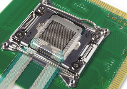
- Heat Sink - Uniform pressure distribution during the mounting of a heat sink is key for performance.
- CMP Wafer Polishing - Improving non-uniformity during the polishing process is a critical goal for manufacturers of wafers.
- Wafer Bonding - An uneven polishing head can cause cracks in the wafer and create product waste.
- Post-CMP PVA Brush Testing - Ensuring proper brush-to-wafer contact pressure and contact area is crucial in achieving clean and particle free wafers.
- Precision Clamping - Unknown clamping forces during computer chip and heat sink mounting or wafer probe testing can cause considerable product defects and quality issues and lead to lower yields, increased costs, and product waste
Looking to improve your process around any of these areas? Contact us to learn more about how pressure mapping data from Tekscan systems can improve semiconductor design and manufacturing at nearly every stage.

Download your free eBook:
Insight from Pressure Mapping into Semiconductor Quality and Manufacturing
Learn more about Pressure Mapping.